ABOUT US
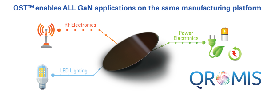
The Company is poised to become one of the premier players in the rapidly growing, multi-billion dollar WBG industry with its disruptive and validated solutions in substrate and device technologies, which enable an unmatched cost, performance, and application scale. Markets served include power electronics, light emitting diodes (LEDs), advanced displays, and RF electronics, and other emerging high performance and energy efficient applications.
As a fabless company, Qromis is driving the commercialization of its unique solutions in conjunction with its foundry network. The Company and its foundry partner offer WBG device foundry services, as well as access to advanced and novel process technology platforms, for its customers and partners.

OUR TECHNOLOGY
A groundbreaking, fab-friendly substrate solution enabling unmatched cost,
performance and application scale for energy-efficient Wide Bandgap Semiconductors
(1) reduce the manufacturing cost,
(2) improve performance and
(3) unlock new applications by enabling access to advanced, state-of-art semiconductor process and device technologies
→ which are serially behind the existing wafer diameter scale and device layers’ quality limitations.
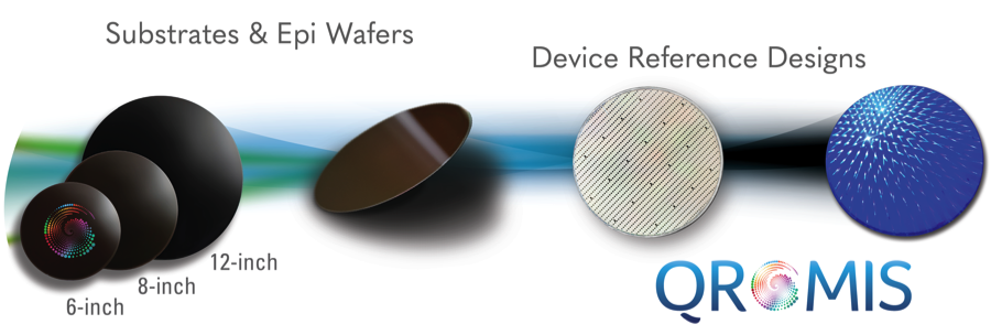
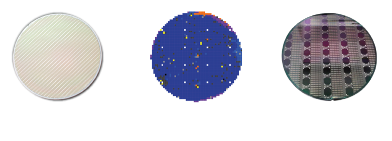
Majority of current fabrication techniques are limited to <6-inch wafers. Efforts to transition to more economical 8-inch wafers, or beyond, and advanced technology platforms have been very challenging despite the significant R&D investments made to date worldwide.
This breakthrough enables scaling:
> to 6-inch, 8-inch and 12-inch diameter, and beyond
> GaN from a few micron thickness to bulk-like thickness on all wafer diameters
> devices from discrete to monolithic and eventually ICs with specifically designed engineered layers starting from QST™ level
The process and integration technologies developed are compatible with existing silicon fabs, eliminating the need for costly development.
Core Technology
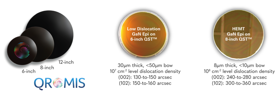
Rather than solving incremental scale and performance challenges of conventional substrates for WBG semiconductors, QST™ has been developed and validated as a disruptive solution, with cross-functional optimization. In this approach, the key properties of substrate material such as stress, lattice mismatch, thermal stability and shape control are engineered independently for the best fit with GaN epitaxial and device layers, as well as with different device architectures and performance targets. QST™ materials layers are integrated together in the conventional semiconductor fab with a simple manufacturing flow.
The resulting large diameter substrates (6-inch, 8-inch, 12-inch or beyond) are capable of supporting from a few to tens of microns of high-quality GaN epitaxy, from which unique, high performance and low cost GaN device structures are fabricated.
A Unique Feature
> High performance devices and applications: fast adoption of advanced modules
> Seamless and fast-cycle transition between 6-inch, 8-inch, and 12-inch
Device Reference Design
> High quality and stress-free GaN,
> Ability to deposit thick, bulk-like GaN epi layers on large diameter substrates,
> Low defectivity, eliminating a major limitation to performance and scalability.
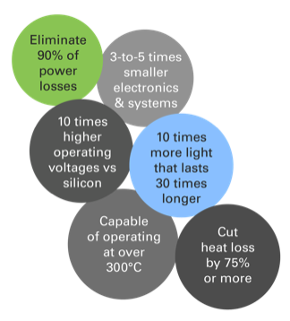
With these distinct features, designers can now break free from the current technological limitations of GaN process technologies and develop advanced device architectures for lateral and vertical device designs of light emitters, switches, rectifiers, as well as monolithic and integrated circuits.
Qromis’ initial reference device designs demonstrate superior performance in high voltage GaN power, high brightness LED and RF communication applications such as switch mode power supplies, motor drives, solid state lighting and base station power amplifiers.
Management Team

Dr. Cem Basceri has spent more than 20 years in materials science and semiconductor technologies with various executive leadership and managerial positions in start-up ventures to Fortune 500 public companies.
Previously, Dr. Basceri served as CTO and Executive Member of Bridgelux, Inc., focusing on energy efficient LED devices, components and smart lighting systems. Prior to that, he served as Senior Director and Chief Technologist in Corporate Development and R&D at Micron Technology, Inc., for more than 10 years (NASDAQ: MU), where he managed the wide bandgap technology development project with $250 Million budget, including the core partnership program at IMEC. Within Micron’s Corporate Development organization, Dr. Basceri lead strategic M&A, partnerships, investments, divestitures and technology licensing deals. He also served as the chair of the Silicon & Systems Group’s Advisory Board and the business unit representative in Micron’s TLP Global Technical Committee. From 2006 to 2008, he lead the SiC materials technology development program at Cree, Inc., (NASDAQ: CREE). From 2004 to 2006, he was involved in a privately-held technology start-up, Intrinsic Semiconductor, which was later acquired by Cree in 2006. During his career, Dr. Basceri managed over $20M in US Government grants and contracts, and worked closely with Department of Energy, DARPA, Air Force, Navy and the Army.
Dr. Basceri has more than 220 issued US patents and number of technical articles in refereed journals. He holds a PhD degree in Materials Science and Engineering (North Carolina State University), and MS/BS degrees in Metallurgical and Materials Engineering (Orta Dogu Teknik Universitesi, Turkey).

Dr. Vladimir Odnoblyudov has spent more than 10 years in optoelectronic and electronic devices, process integration and wide bandgap semiconductor technologies with executive leadership and technical management positions, from early stage start-ups to Fortune 500 companies.
Dr. Odnoblyudov served as Director of R&D and Emerging Technologies of Bridgelux, Inc., focusing on next generation solid state lighting (SSL) technologies, from LED chip level through smart sub-system level. Before that, he served as Director of LED Solutions at Micron Technology, Inc., (NASDAQ: MU), leading R&D efforts for revolutionary large diameter GaN wafer and device technology in 200mm CMOS pilot line fab, and with $50 Million annual budget. Development and pilot line activities spanned from substrate level through backend including chip-scale packaging and applications development. Within Micron’s R&D organization, Dr. Odnoblyudov served as a member of the IP Review and Development Committee. Prior to that, from 2009 to 2010, he was the Founder and President of Meranna, Inc., focusing on IP development of new vertically integrated SSL solutions. From 2006 to 2009, he was the Founder and CTO of Quanlight, Inc., an LED start-up focusing on development of novel yellow-red chip technology which drew several rounds of corporate and venture financing.
Dr. Odnoblyudov has more than 60 issued and pending US patents and >30 articles in referred journals and conference presentations. He holds a PhD degree in Applied Physics (University of California San Diego, Department of Electrical and Computer Engineering), and MS/BS degrees in Solid State Physics (Saint-Petersburg State Technical University, Russia). While obtaining MS/BS degrees from SPbTU, Dr. Odnoblyudov worked as Research Assistant in the Laboratory of Semiconductor Heterostructures, lead by Prof. Zhores Alferov, Nobel Prize Winner in Physics in 2000 (Ioffe Physico-Technical Institute).

Mr. Hamid Emarlou has more than 30 years of experience in advanced electronics technologies with various executive and leadership positions focusing on product development and manufacturing operations, extending from start-ups to Fortune 500 companies. He served as Vice President of Worldwide Operations at Wyse Technology, the global leader in cloud client computing, which was later acquired by Dell. Mr. Emarlou also held a number of executive and leadership positions at Solectron Corporation (later acquired by Flextronics International, Ltd. in 2007), a global electronics manufacturing company for original equipment manufacturers (OEMs).
Mr. Emarlou received his bachelor degree in Electrical Engineering Department of San Jose State University. He also completed the Executive Development Program at Kennedy School of Business at Harvard. He was a Board Member of the Associated Industries of Massachusetts and Center for Quality Management during 2000-2003, as well as the Advisory Board Member of the Engineering Department of Boston University during 2001-2003.

With over 25 years of legal experience advising high-tech companies in Silicon Valley, Gabriel Sandoval most recently Chief Legal Officer of Deem overseeing Deem's legal department and the founder and CEO’s key advisor. Throughout his tenure at Deem Gabriel was instrumental in all critical aspects of the company overseeing M&A, capital fund raising, corporate strategy and business development, among other areas. Prior to joining Deem, Gabriel was vice president and general counsel at Ariba where he was responsible for all worldwide legal functions from the time the company was an emerging e-Commerce business through its IPO. Prior to Ariba, Gabriel was corporate counsel at Oracle Corporation negotiating Oracle's software licensing agreements; strategic alliance, ISV and OEM agreements; and joint development and marketing agreements. Fluent in English and Spanish, Gabriel for a period also managed legal for Oracle's Latin American division and ultimately oversaw Oracle's financial services vertical across North America. Before becoming an in-house corporate attorney, Gabriel was a business associate at Ropers, Majeski, Kohn, & Bentley.
Gabriel earned a BA in Economics from Stanford University and a JD from the Santa Clara University School of Law. He is a member of the State Bar of California and the Santa Clara County Bar Association.

Mike Noonen leads sales and business development at Silego Technology, the leader in Configurable Mixed-Signal. He has 25 years of experience of growing top and bottom lines and mixed-signal innovation. Most recently he was the interim CEO and Board Director at Ambiq Micro. Previously, Noonen was the Chairman and co-founder of Silicon Catalyst, the semiconductor solution start-up incubator based in Silicon Valley. Silicon Catalyst won the 2015 EE Times/EDN “Start-up of the Year” Ace Award.
While EVP, Global Products, Design, Sales, & Marketing at GlobalFoundries, Noonen led the customer focused turnaround that resulted in industry leading growth in 2012. In 2008 Noonen joined NXP following its spin-out from Philips. As EVP, Worldwide Sales & Marketing, he and NXP's CTO crafted NXP's high performance mixed-signal repositioning leading to its growth and 2010 IPO.
Noonen has held GM and executive sales and marketing roles at National Semiconductor, Cisco Systems and 8x8. He started his career at NCR Microelectronics as an FAE teaching mixed-signal ASIC design. He holds a BSEE from Colorado State University and in 2012 was named the College of Engineering Distinguished Alumni. He also served on the Global Semiconductor Alliance Board of Directors and was Chairman of Socle in Taiwan. He holds multiple patents in the areas of Internet telephony and video communications.

In his 20 years career at NEC, Mr. Mukaibayashi has built the experience in application engineering, marketing and business strategy for the system LSI. He played key roles in product definition and business strategy. During his time in the Silicon Valley from 1991 to 1998, he produced and implemented several strategic alliances and M&A, and incubated start up companies many of which achieved successful exit. Based on well balanced experience and knowledge in engineering, marketing and intellectual property rights, he produces strategic collaboration between portfolio companies and major Japanese companies. He is also on a technical committee of NEDO, a governmental organization.
Want to learn more about Qromis?
We would like to hear from you.
info@qromis.com
Qromis, Inc.
2306 Walsh Ave
Santa Clara, California, 95051
United States